Table of Contents
Diary
Future:
2018-04-17
We made initial schematic in kicad.
Next define electric bla bla in pcm3168A component. Make sure that every pins are connected to something (mark unused as unused). Continue until electrical rule check is passed.
When this is done figure out how to make PCB.
2018-02-27
We (re)started working with kicad to define the PCM and FPGA chips.
Information about the component library file format: http://kicad-pcb.org/help/file-formats/
We are considering using the iCE40 Ultra (iCE5LP4K) instead of the iCE40HX8K.
2018-01-23
Somewthing about blocking and non-blocking assignment in verilog:
Today we decided that Verilog sucks and added vhd2vl to toolchain.
Next time we will implement shiftregister in vhdl.
2018-01-16
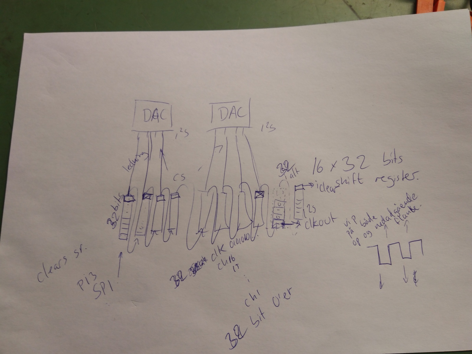
Today we got two FPGAs working together as a serial coupled shift register. (The working code has been committed to git.)
Next time we will double the clock rate output from the first to the second.
2017-12-26
Today we got it working. Now we have a working shiftregister. We tried to serial couple another fpga, but couldn't make the clock output work as expected.
Next we want to use the second fpga to emulate the CODECs and the channel reset mechanism. Maybe also try to make the shift register as a module so we can 'stack' them.
2017-12-19
Today we had the fpga tool-chain working. Next time Jonas will bring his PSU…
We experimented with a shift register implementation. Didn't get it working though…
Next time we will make it work! Analyse clock and MOSI signals with scope. As a home assignment, read up on Verilog timing.
2017-12-12
Verilog short introduction: http://www.doe.carleton.ca/~jknight/97.478/PetervrlK.pdf
iCEcube user guide: http://www.latticesemi.com/~/media/LatticeSemi/Documents/UserManuals/EI/iCEcube201701UserGuide.pdf
Today we created a build script for creation of the fpga build environment (icestorm toolchain), located in the dginabox/fpga-toolchain/ folder.
Next time we create a Verilog program that reads a single byte from SPI and sets the corresponding bits on the 8 LEDs.
2017-12-05
Verilog cheat sheet: https://www.cl.cam.ac.uk/teaching/0910/ECAD+Arch/files/verilogcheatsheet.pdf
Started to write build.sh script for building icestorm tools. (out-of-tree builds)
Connected gpio4 to C16 input on fpga and wrote a program that used C16 as clock.
Experimented with verilog syntax.
Read Jonas' laptop Makefile for blinky for instructions on how to build blinky.
2017-11-14
Today we did: Made connector for SPI interface for easier access. Located most of the SPI pins on the iCE40 eval board.
Looked briefly at: https://hackaday.com/2017/04/13/lattice-ice40-fpga-configured-by-linux-kernel/
Next time we plan to: Read up (homework) on the eval board schematics documentation.
2017-11-07
Today we did: Connected Saleae to RPI and verified that the burst.c seem to be able to write to the SPI bus on he RPi3.
Suggestion for alternative FPGA with more RAM: iCE40UP5K
SPI prog flow: Page 20 or Appendix A in iCE40 Configuration and Programming.
Sync word in bitstream:
7E AA 99 7E
Next time we plan to: Find the SPI (MISO, MOSI, CLK and CS), SPI_SS_B, CRESET_B and CDONE pins on the iCE40 eval board and make suitable connector.
2017-10-17
Today we did:
- Connect to the RPi3 (it is configured with static IP 10.0.0.1)
- Built native SDK for the RPi3 (“bitbake -c populate_sdk core-image-minimal” in the yocto VM).
- 64 bit only - so not on “Merde”…
iCE40 Configuration and Programming
Do NOT write to NVCM. It is a one time only write!
RPi3 PIN header: image
Next time we plan to: Bring saleae and make burst run on the RPi (set up SPI and GPIOs).
2017-10-10
Today we did: Compile a blinky program with the open source yosys toolchain and upload and run on FPGA.
Next time we plan to: Setup pi ice40 toolchain and upload the program via SPI.
2017-10-03
We received the FPGA eval kit for the iCE40HX8K chip.
The FPGA has 128kbit memory, which will result in 2048 samples buffer clock-out via SPI followed by approx 9ms sleep (controlled by interrupt from the FPGA)
The chip is not easy to solder, so we are considering using two 80kbit QFN chips instead, in daisy chain, handling 8 channels each.
